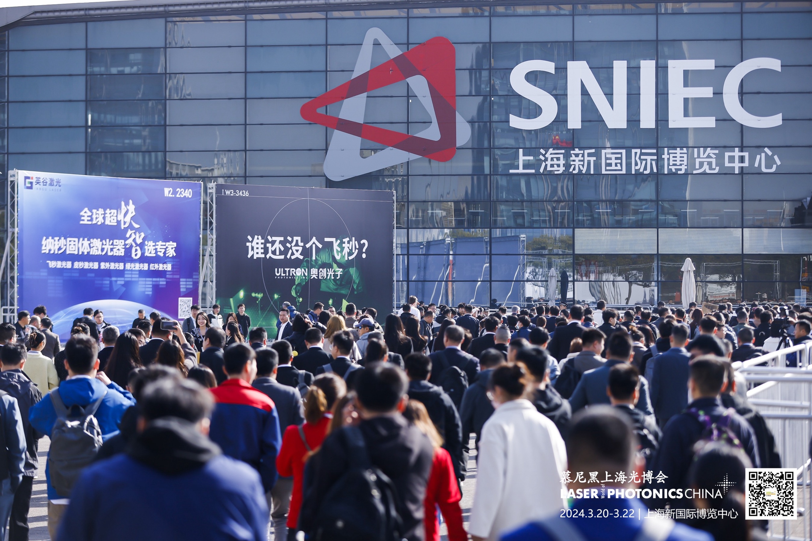
A Spirit of Optimism in China: LASER World of PHOTONICS CHINA and SEMICON China attracted huge interest

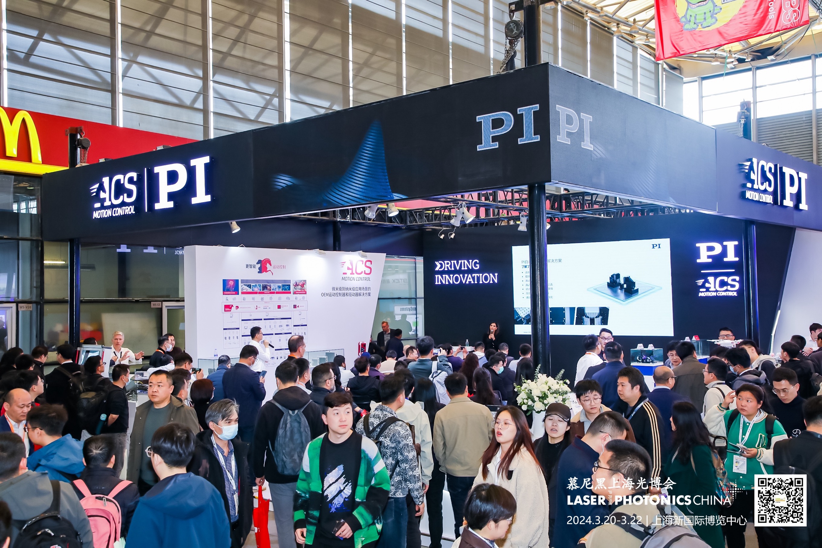
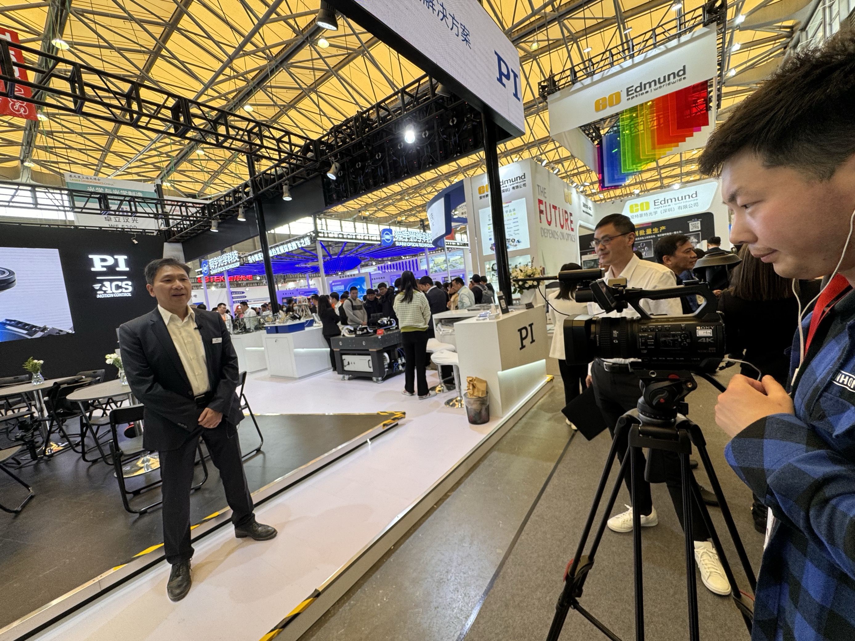
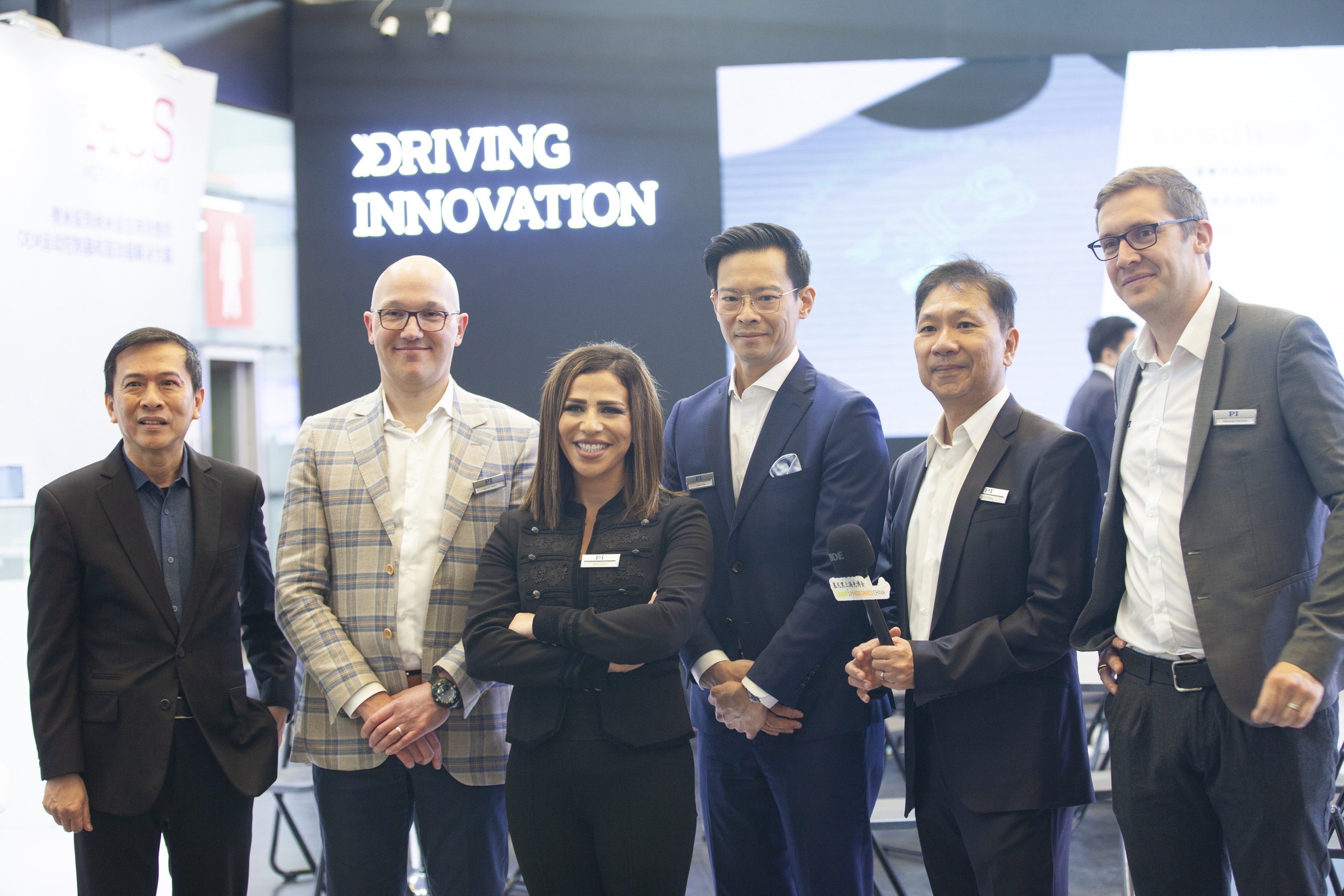
LASER World of PHOTONICS CHINA and SEMICON China, Asia's leading trade fairs for optical technologies as well as semiconductor manufacturing, took place in Shanghai in mid-March. PI was represented with a large joint stand with ACS.
Hsin Chia, PI’s Director of Sales APAC, was highly satisfied with the results of our trade fair appearance: “The show was a great success for PI China and ACS, and therefore for the PI Group as a whole. We received more than 300 leads, including several for our new technology demonstrator for film metrology in semiconductor manufacturing. At least as important is the high visibility of the PI brand, which we continued to build through numerous interviews, lectures, and presentations.”
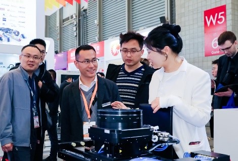
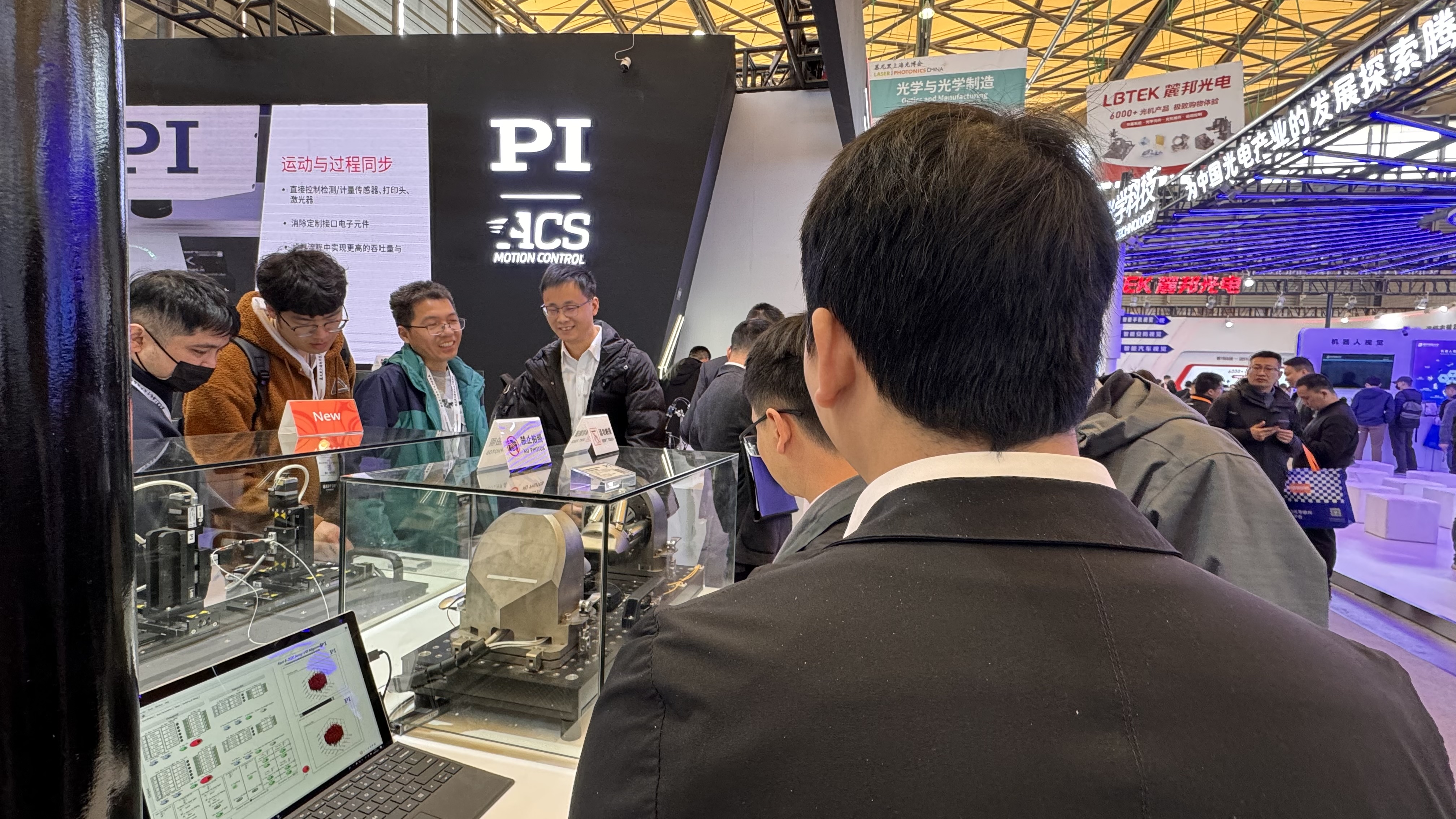
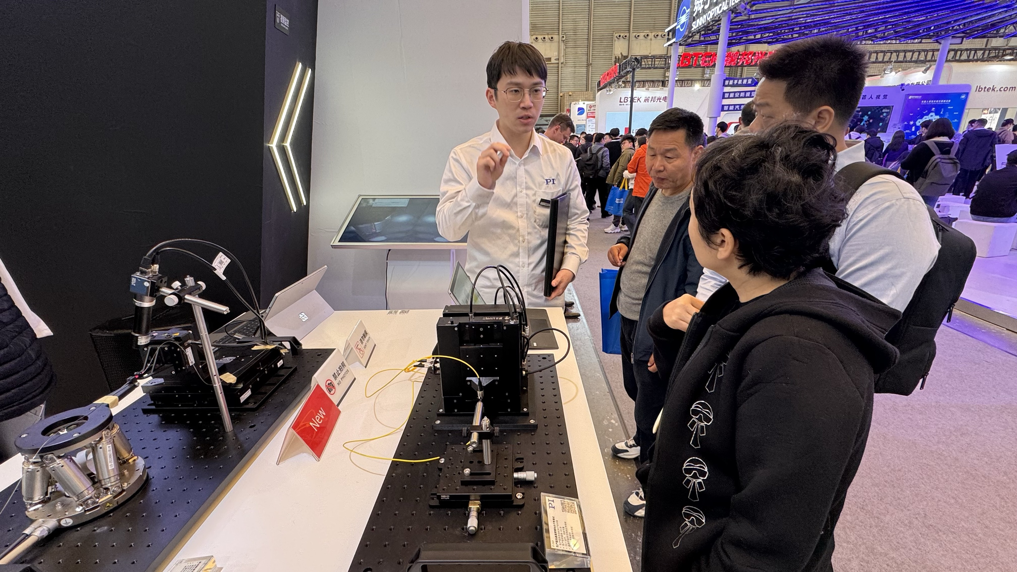
The technology demonstrator for film metrology in semiconductor manufacturing attracted a lot of attention.
PI already has an excellent reputation in China for technology leadership and product performance. This position is strengthened by the fact that we have our own technology development and production facilities in China. “Made in China for China is the motto here, which is rewarded by the market,” affirms Laurent Melin, SVP Sales Global. Examples include various linear stages and the stacked fiber alignment system F-836 based on L-836 linear stages. Air bearings developed at our plant in Changzhou, China, were also shown at the trade fair for the first time. Additionally, the aforementioned technology demonstrator, which was developed as part of the PI Metro project, is designed and manufactured at our Changzhou plant.
At the PI stand, our colleagues presented our portfolio, including these innovations, to over 1,800 visitors who stopped by. PI's new technologies were very well received by the visitors. Three innovations for our core market segments “Semiconductor” and “Photonics” took center stage of the presentation:
- PILightning & FMPA (Fast Multi-Channel Photonics Alignment): a new first light search algorithm for photonics alignment applications.
- Photonic alignment toolkit: an extension of the suite of mechanical solutions to better address different application needs.
- Technology demonstrator for a motion platform for film metrology in wafer inspection, designed to trigger customer projects in film metrology and related metrology applications.
With these important innovations, PI is positioning itself precisely where its core competencies lie: “One focus of our trade show appearance was on motion and positioning solutions for the semiconductor market. This is where our core competencies, namely Nano Positioning, Piezo Technology, and Performance Automation, really come into their own. The new technology demonstrator for film metrology in wafer inspection is a good example of the customer-oriented and application-oriented implementation of these core competencies,” states Hsin Chia.
As our main segments are in highly competitive industries, such trade fair appearances and presentations of innovations are even more important. Laurent Melin points out: “Photonics and semiconductor applications are among the most innovative technologies in the world. As a leading provider of precise positioning solutions, PI has consistently pushed the boundaries of what is technically feasible. We are working closely together with machine builders and system integrators, and in addition, we are a member of interdisciplinary research initiatives all over the world.”
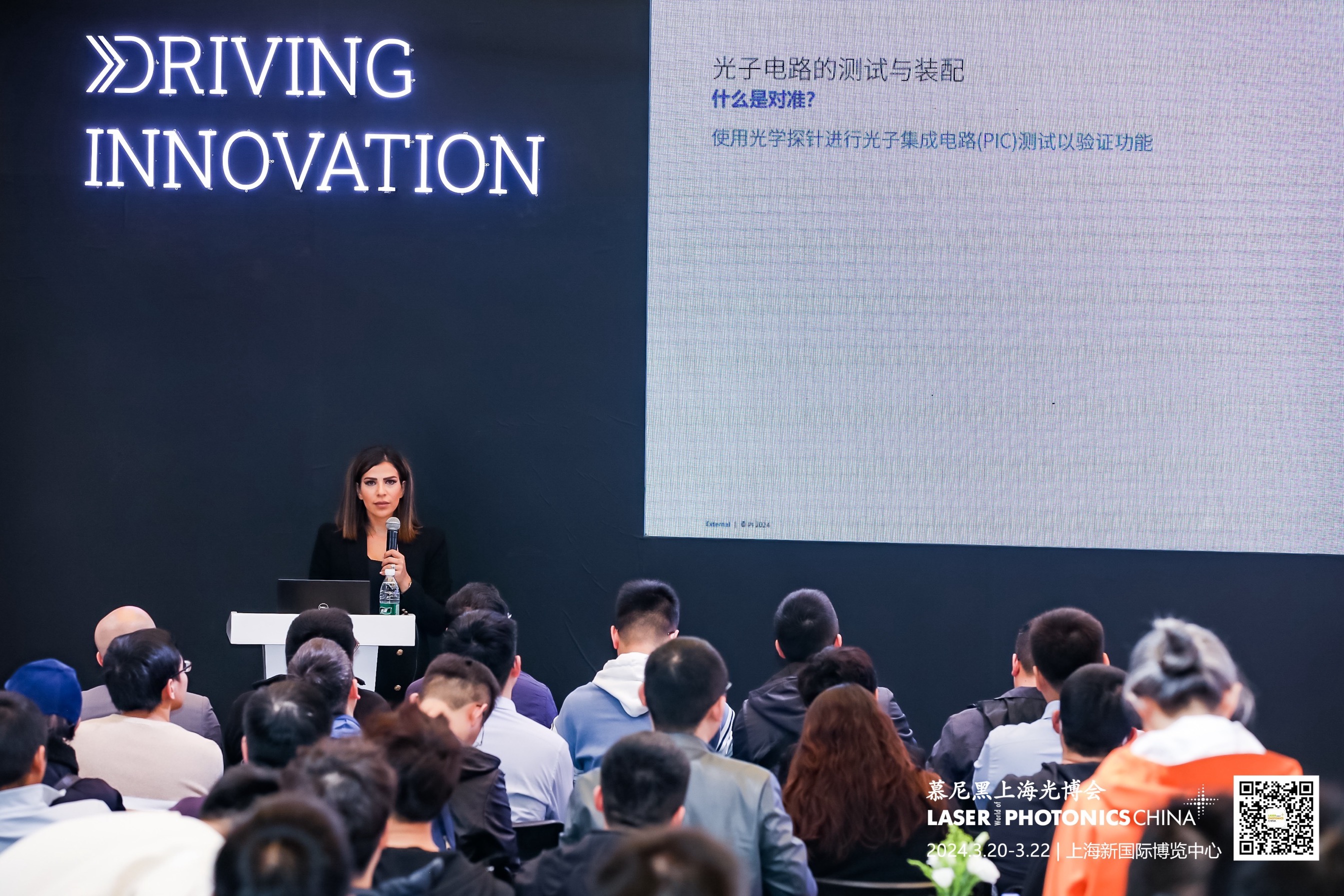
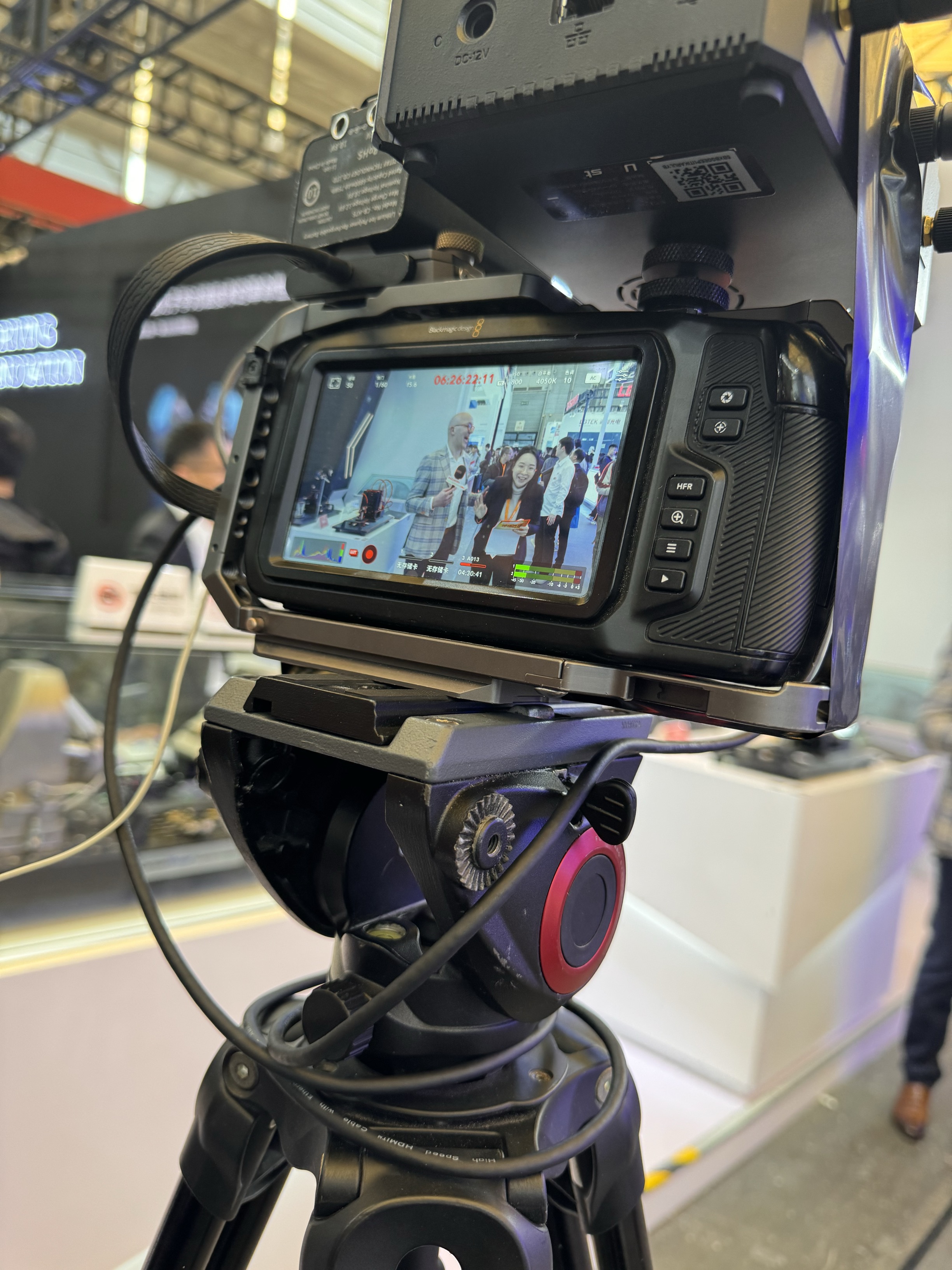
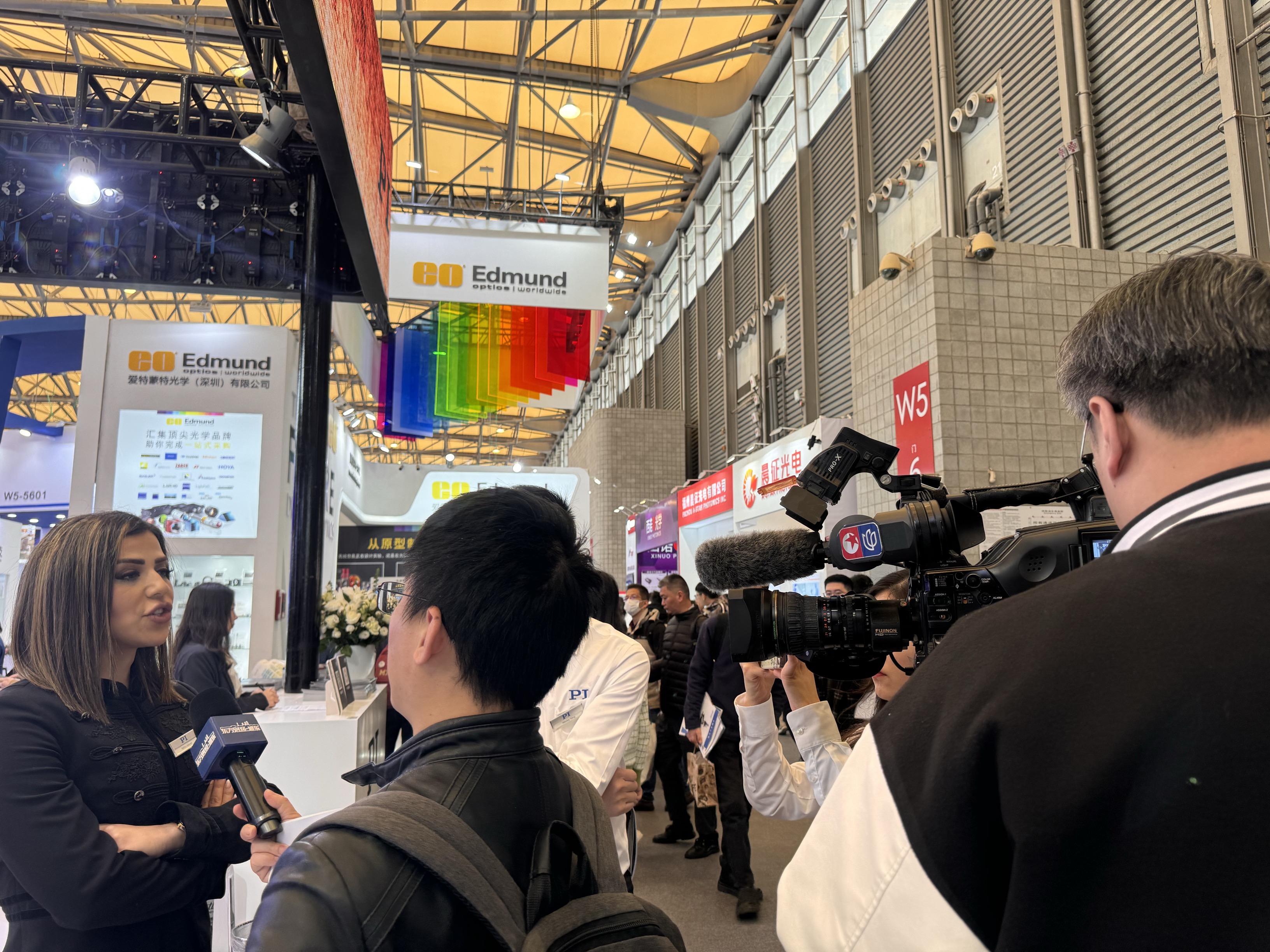
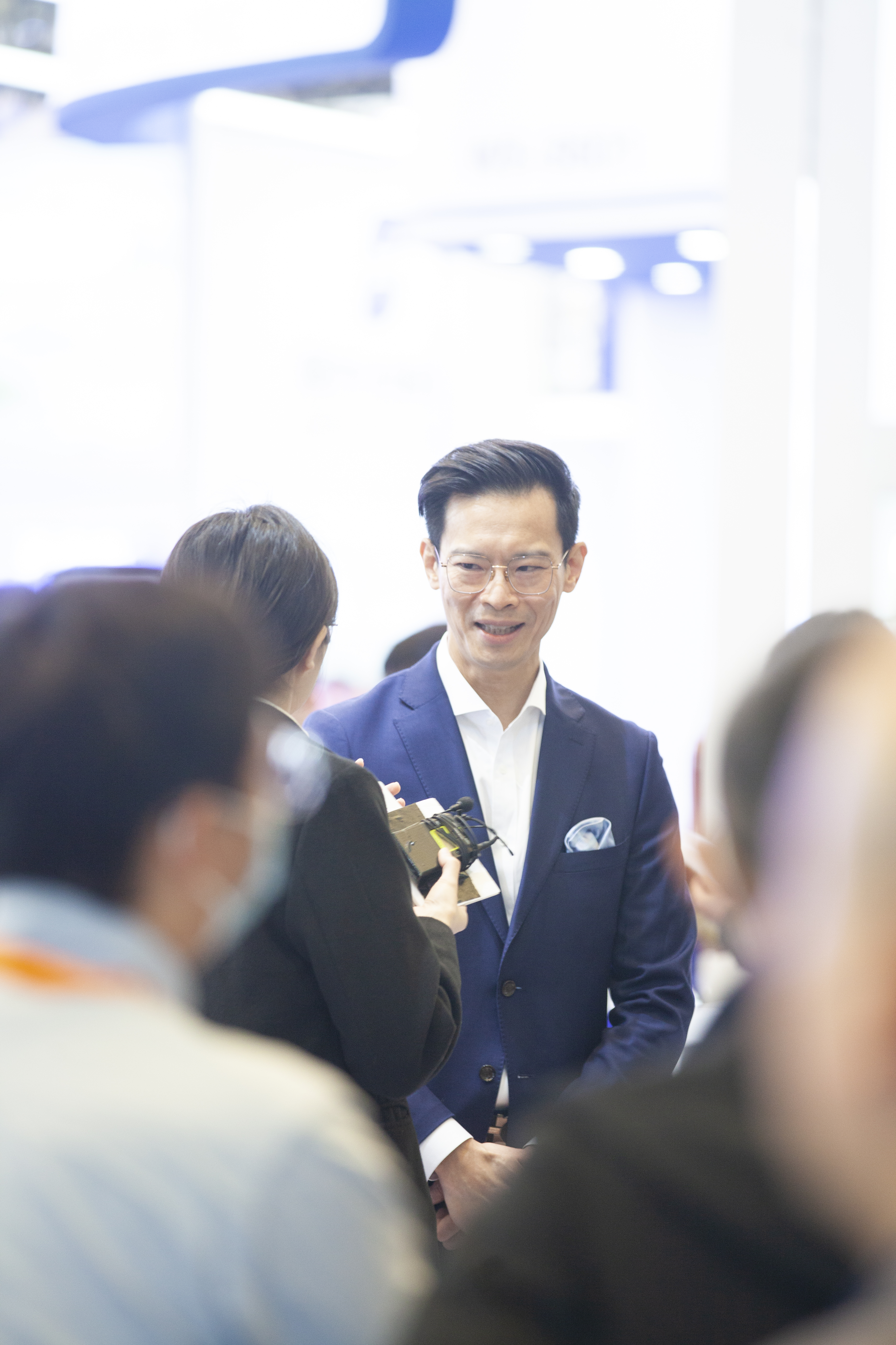
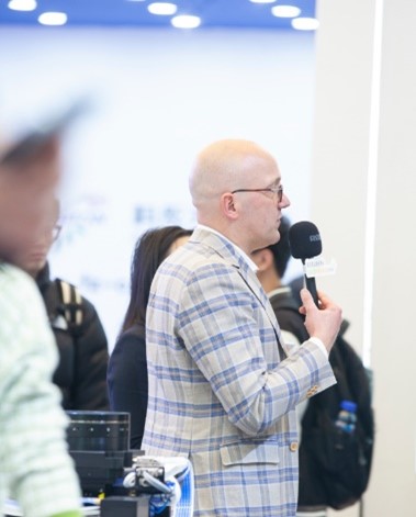
In addition to the product and technology innovations, the interviews with Hsin Chia, Laurent Melin, Chris Hong, and Derek Ling attracted a lot of attention. Nikta Jalayer was invited to give a TV interview, which generated additional interest. The technology presentations and lectures by Derek Ling, Nikta Jalayer, and Kai Shen (ACS) were very well received by the audience of over 200 people.
Interview with Laurent Melin
The response to our presence at the show far exceeded our expectations. This is an impressive confirmation that we are on the right track with our focus on semiconductor and photonics and that we have correctly identified the particular growth opportunities in the Asian and especially the Chinese market.
Background:
There are strong efforts in China to achieve greater self-sufficiency in semiconductor manufacturing. The Semiconductor Equipment and Materials International (SEMI) trade association reports that, in 2023, the investment volume for semiconductor equipment and materials in China exceeded 30 billion USD. This investment volume is larger than the combined spending of Europe, Japan, and North America in the same year. In addition, the 23 % increase in investment in China compared to 2022 was the largest globally. The great opportunities that this alone creates for PI are further enhanced by the fact that we have our own development and production facilities in China.