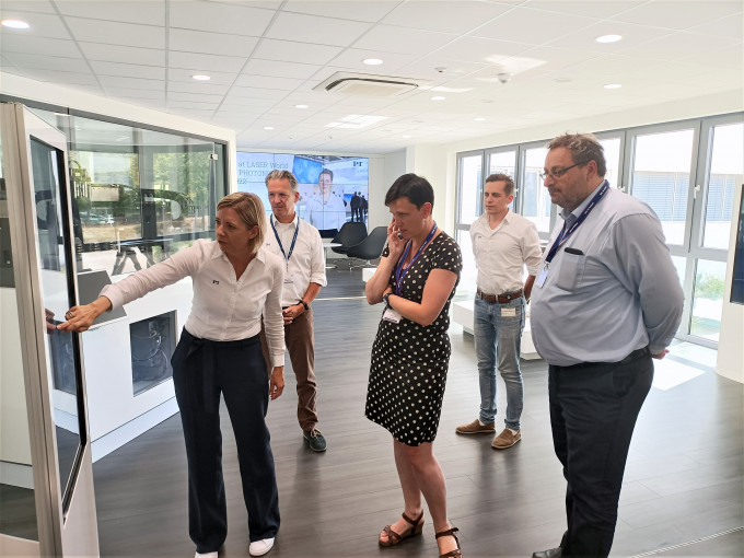
CITC Visits PI in Karlsruhe - Focus On Closer Cooperation on Marketing Topics
Dear colleagues,
on Tuesday, August 16, 2022 we had a visit from Marco Koelink, Business Development Manager, and Christian Ketelaars, Marketing & Communication Officer, both from CITC.
CITC is an independent "non-profit" research center in Nijmegen, Netherlands, that develops packaging solutions for semiconductor devices and photonic devices (= silicon photonics and photonic integrated circuits). With its 17 employees, CITC acts as a multiplier for Packaging Solutions and has Europe-wide contacts in the photonics scene. Of particular interest to PI is the fact that CITC relies on our fiber alignment systems (F-712) for its development projects in the field of photonic packaging.
Through its international networking, CITC is also heavily involved in discussions about the future of photonics, both on the application side and technologically. In addition to getting to know each other better, one goal of CITC's visit was to discuss current market and technology developments and to establish a regular exchange. To this end, it was valuable that we were also able to demonstrate new solutions for fiber alignment in the photonics laboratory.
Another focus was the development of ideas and ways in which we can better communicate the respective competencies and customer benefits of the solutions in the market. There are many starting points here that go far beyond pure marketing communication.
Marco Koelink and Christian Ketelaars were enthusiastic about what they could see at our company and were very impressed by the technological diversity and the extensive competencies at PI.
A special thank you goes to Marco Vogel, Manager Production Management Hexapods, for the great factory tour and to Sonja Stoll from Application Development for demonstrating the new fiber alignment solution based on stacked linear axes and ACS controllers.
Background: Why is CITC's work so significant?
Every new photonics chip requires its own "recipe" for interconnection with signal-carrying optical fibers and subsequent packaging (also called "housing"). There are several reasons for this: The great diversity in chip design, the use of a wide variety of substrate materials, and the large number of different elements on the chip, such as laser diodes, photodiodes, and planar waveguides. Taken together, these boundary conditions each require different approaches to coupling and packaging. The flexibility and efficiency of our fiber alignment solution is particularly helpful here - and is not only used by CITC in process development, but also recommended to the respective customer as part of the solution.
Best regards
Sander Slagter
Engineer Technical Sales
